A Scanning Electron Microscope is a game-changer in the world of imaging. Imagine the ability to zoom in on an object so closely that even the tiniest details come alive in stunning clarity. That is what SEM does. But how does it work? Let’s break it down.
An SEM uses a beam of electrons instead of light to look at the surface of a sample. The electrons work with the atoms in the sample to make signals that form an image. Unlike regular optical microscopes that use light, SEM can show much finer details—up to 100,000 times bigger! This means you could see the surface of a cell and even look at individual molecules. That’s pretty amazing, isn’t it?
What really makes the SEM special is the level of detail it provides. The electrons are traveling over the surface of the object and then bouncing back to make clear, 3D images. Think about studying a tiny bug: you’re not just going to see its legs but the fine texture of its shell in great depth and clarity.
The problem is there, though. The SEM can’t tell you what’s inside your specimens. It only shows you the surface. That’s an enormously valuable thing for researchers and scientists. Whether you’re studying materials, biological samples, checking for cracks in a metal surface, it gives you information you can’t get with a regular microscope.
It can be a great curiosity spark in the classroom or lab. Do you ever wonder what things look like at the molecular level? SEM lets you see them in fine detail. In fact, it has revolutionized fields such as material science, biology, and even archaeology!
Now, I don’t mean to mislead you—SEM is not something to take lightly. It is a special tool that needs careful use and specific ways to prepare samples. For instance, biological samples must be covered with a thin layer of metal, because electrons do not go through air easily. You can’t just place a sample under an SEM and hope for amazing results. It requires practice.
Even with difficulties, once you understand it, SEM imaging can be a very interesting way to look at tiny things. It’s like opening a door to a new way of seeing, showing hidden parts of reality that we couldn’t see before. It’s not just science; it’s science that feels amazing.
So, next time you’re studying materials or exploring the microscopic world, remember: the Scanning Electron Microscope isn’t just a tool, it’s a portal into a universe so small, it might just blow your mind!
Definition of Scanning Electron Microscope (SEM)
SEM is a form of microscope which uses focused beams of electrons to view the surface of a sample. It produces very detailed images of the surface structure at a very high zoom level.
In 1937, Mafred von Ardenne built the first Scanning Electron Microscope to outperform the transmission electron Microscope. He scanned a small raster with high-resolution power, which was made using a beam of electrons focused on the raster. He also intended to reduce the problems of chromatic aberrations images produced by the Transmission electron Microscopes. Scientists and research institutions made more studies. One of the companies was the Cambridge Scientific Instrument Company. In 1965, they were able to make a whole Scanning Electron Microscope known as Stereoscan. A Scanning Electron Microscope cost around $1 million.
A Scanning Electron Microscope (SEM) is a kind of electron microscope that looks at the surfaces of tiny living things. It uses a low-energy beam of electrons to focus on and scan the samples. Electron microscopes were created because light microscopes were not very efficient. Electron microscopes have much shorter wavelengths than light microscopes, which gives them better ability to see details.
Principle of Scanning Electron Microscope (SEM)
It functions by the collision of electrons and the surface of a sample to produce signals in the form of detailed images as well as information about the sample. In comparison, TEM takes advantage of the transmitted electrons while studying the sample. SEM studies the surface of the sample with the use of emitted electrons.
The focused electron beam will affect the specimen, leading to different types of electrons that come from the surface. They include secondary electrons, backscattered electrons, and diffracted backscattered electrons. Each of the emitted electrons contributes to forming the image.
The secondary electrons mainly allow us to see the shape and surface features of the material. Since they have low energy, they come from the top layers of the sample and provide us with minute information about the surface. On the other hand, the backscattered electrons, being more energetic, provide us with information about what the material is made of. The strength of the former is a function of the atomic number of the elements involved, helping to create differences in the final image.
In SEM, the electron beam travels in a grid pattern over the specimen. Upon hitting the surface, different signals are picked up and processed to create an image. This detailed imaging method enables researchers to view the small details of a specimen’s surface at a microscopic level, and it is, therefore, quite useful for material science, biological samples, and nanostructures.
So, SEM can create images of shapes, structures, and materials using electrons that it emits. It is a useful and important tool for scientific research.
How does the Scanning Electron Microscope (SEM) work?
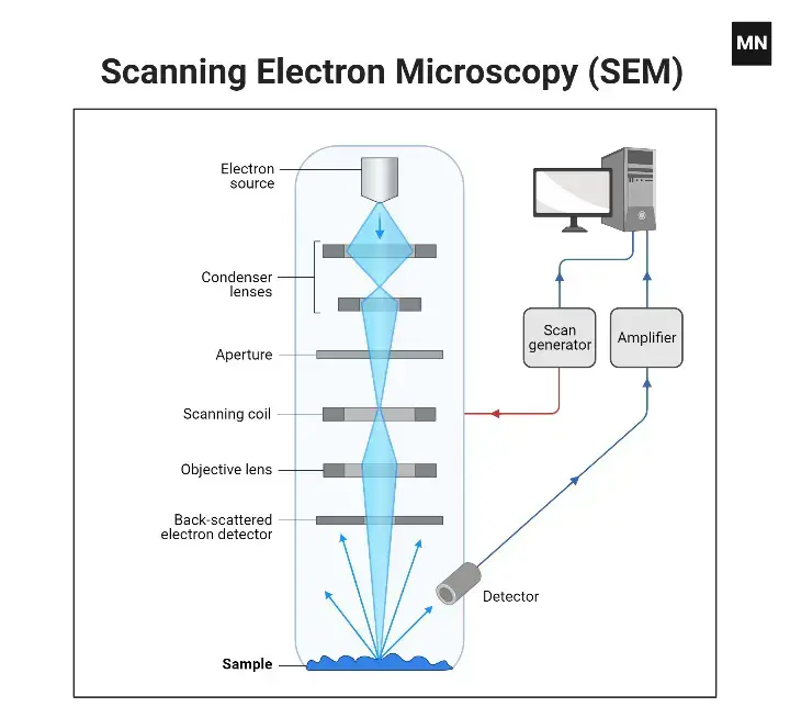
- Electron source and electromagnetic lenses – Tungsten filament lamps are used here as electron emitters. They stand at the top of the column similar to those being used in transmission electron microscopy. Electron emission – The thermal energy applied to the source causes the electrons to move rapidly toward the positively charged anode.
- Interaction with the specimen– The electron beam generates primary (high energy) and secondary (low energy) electrons, which give information on the topography of the specimen’s surface and its composition.
- Specimen treatment– Most samples, including air-dried ones, can be examined directly, but microbial specimens require fixation, dehydration, and drying to preserve structure and prevent collapse in the vacuum.
- Sample preparation—The specimen is attached and coated with a thin layer of heavy metals to increase electron scattering and improve the resolution of the image.
- Scanning process—The electron beam is scanned in a back-and-forth motion across the specimen. Secondary electrons are emitted from the surface of the specimen due to the interaction of the beam with it.
- Secondary electron detection– The secondary electrons are trapped by a special detector where they hit a scintillator that produces light that is converted into an electric current to produce an image.
- Image production– The current is transmitted to the cathode ray tube to create an image that is like a television picture, and can be viewed and photographed.
- Surface contrast– The raised surfaces emit more secondary electrons, which appear brighter on the screen, while the depressed surfaces emit fewer electrons, which appear darker.
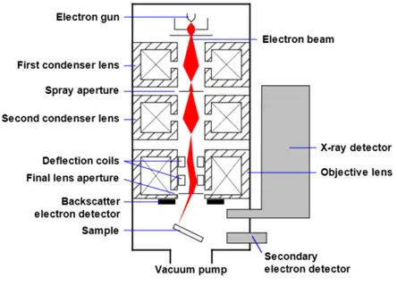
Parts of a Scanning Electron Microscope
The key components of a Scanning Electron Microscope (SEM) include:
- Electron Source- This is essentially the source of electrons. These are generated using thermal heat and at a voltage of 1 to 40 kV. These electrons are gathered into a focused beam that is utilized afterward in imaging and analysis processes. There are three primary types of electron sources available for use: Tungsten filament, Lanthanum hexaboride, and the Field Emission Gun (FEG).
- Lenses– The SEM has several condenser lenses that concentrate the electron beam emanating from the source through the column. This results in a narrow beam of electrons that gives a spot known as the “spot size.”
- Scanning Coil- The scanning coil is used in deflecting the electron beam along the surface of the specimen, thus enabling scanning and imaging.
- Detector– The detector system consists of several detectors which are capable of detecting secondary electrons, backscattered electrons, and diffracted backscattered electrons. Voltage speed and the specimen density may influence how well these detectors will perform.
- Display Device (Data Output Devices)– The display device, or simply put, the output data device performs a very crucial role in data presentation associated with the scanning procedure. It facilitates in the visualization and analysis of the specimen.
- Power Supply- This component provides the power necessary to supply the electrical energy that will run through all components within the scanning electron microscope.
- Vacuum System- The vacuum system establishes and sustains a low-pressure environment within the SEM, which is crucial for optimal electron beam performance as well as avoiding interference with the imaging process.
Applications of the Scanning Electron Microscope (SEM)
- Materials Science- They are widely applied to study surface morphology and composition of materials in the development and quality control of metals, polymers, ceramics, and composites.
- Biology and Medicine- SEMs help in the study of cell structures, tissues, and microorganisms with respect to their morphology and their interactions. SEMs help identify diseases and viruses, test new vaccinations and medicines, and compare tissue samples of patients in the control and test groups.
- Geology and Mineralogy- SEMs are used in the study of mineral composition, texture, and structure in order to gain knowledge on geologic formations and the discovery of natural resources.
- Forensic Science- During forensic investigations, SEMs are used in the examination of gunshot residues and trace evidence including microscopic particles leading to criminal investigation and judicial processes.
- Nanotechnology- SEMs are crucial for the development and characterization of nanomaterials, providing the ability to visualize and analyze structures at the nanolevel, an absolutely fundamental step toward applications of nanotechnology.
Advantages of the Scanning Electron Microscope (SEM)
- High Resolution and Magnification- SEMs provide very high imaging resolution, which makes it possible to visualize surface details at the nanometer scale. This capability makes it possible to examine fine surface structures and microstructures with very high clarity.
- Three-Dimensional Imaging- The large depth of field inherent to SEMs gives images a three-dimensional appearance and significantly enhances our perception of the topography of samples.
- Elemental Analysis- The addition of EDS enables SEMs to perform qualitative and quantitative elemental analyses. This is an essential capability used in identifying material compositions and detecting foreign materials.
- Versatility in Sample Analysis- SEMs can analyze a wide variety of sample types, including metals, polymers, ceramics, and biological specimens. This versatility makes them valuable across diverse research and industrial applications.
- Non-Destructive Testing- The scanning process in SEMs is non-destructive, allowing for repeated analysis of the same sample without altering its structure. This is particularly advantageous in quality control and failure analysis.
- Large depth of field– SEMs have a large depth of field so that more of the specimen is in focus at any one time. This feature is useful in studying specimens whose surfaces have various topographies.
Limitations of the Scanning Electron Microscope (SEM)
- The costs of purchasing and maintaining SEMs are quite high. The intricate technology and various components lead to considerable initial expenses, and routine maintenance is crucial to uphold their peak performance.
- Sample Preparation Requirements- Samples may be lightly coated with a conductive material, for example, gold or carbon to prevent charging under the electron beam. This is a laborious preparation procedure that also introduces artifacts unintentionally.
- Vacuum Environment Limitations- Scanning Electron Microscopes operate in a vacuum, which may limit the type of samples that can be studied. For example, wet biological samples may require special preparation or are simply too wet to be imaged by SEM.
- Risk of Sample Damage- The electron beam can damage sensitive samples, especially organic or biological samples. Electrons can catalyze chemical reactions, alter structures, deform, or even break samples.
- Limited Information on Internal Structure- SEMs are mainly sensitive to the topography and chemistry at the surface of samples. Generally, they can offer very limited or no information about the structure inside unless a sample is prepared with careful sectioning. This may not be possible with all materials.
- Size and Space Requirements- SEMs are large instruments that take up much space. Ideally, they are placed in an environment free of electrical, magnetic, or vibrational interference in order to maximize image quality.
- Training and Expertise- The operation of an SEM demands thorough training in understanding the subtle nuances of the working of the machine and the basic principles of electron microscopy. It is crucial for high-quality images and avoiding damage to the microscope.
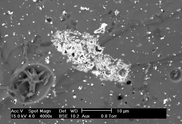
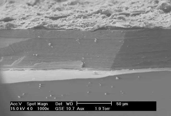
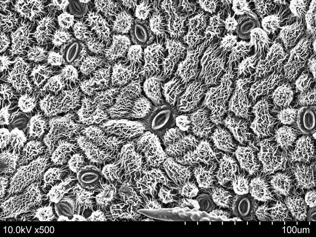
Scanning Electron Microscope (SEM) Images

- https://www.microscopemaster.com/scanning-electron-microscope.html
- https://www.atascientific.com.au/sem-imaging-applications-practical-uses-scanning-electron-microscopes/
- https://www.nanoscience.com/techniques/scanning-electron-microscopy/
- https://cf.gu.se/english/centre_for_cellular_imaging/electron-microscopy-
- https://en.wikipedia.org/wiki/Scanning_electron_microscope
- https://www.britannica.com/technology/high-voltage-electron-microscope
- https://www.frontiersin.org/articles/10.3389/fmicb.2020.02014/full
- https://www.atascientific.com.au/sem-imaging-applications-practical-uses-scanning-electron-microscopes/